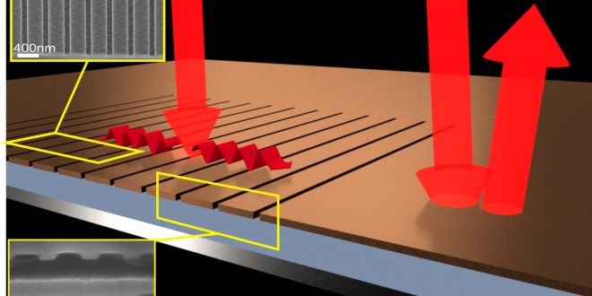
A breakthrough by Australian scientists could make infra-red technology easy-to-use and cheap, potentially saving millions of dollars in defence and other areas using sensing devices. The study has demonstrated a jump in the absorption efficiency of light in a layer of semiconductor that is only a few hundred atoms thick – to almost 99 percent light absorption from the current inefficient 7.7 percent.
Infra-red devices are used for improved vision through fog and for night vision and for observations not possible with visible light; high-quality detectors cost approximately $100,000 (including the device at the University of Sydney) some require cooling to -200°C.
Now, research spearheaded by researchers at the University of Sydney has demonstrated a dramatic increase in the absorption efficiency of light in a layer of semiconductor that is only a few hundred atoms thick – to almost 99 percent light absorption from the current inefficient 7.7 percent.
Co-author from the University of Sydney’s School of Physics, Professor Martijn de Sterke, said the team discovered perfect thin film light absorbers could be created simply by etching grooves into them.
“Conventional absorbers add bulk and cost to the infrared detector as well as the need for continuous power to keep the temperature down. The ultrathin absorbers can reduce these drawbacks,” Professor de Sterke said.
“By etching thin grooves in the film, the light is directed sideways and almost all of it is absorbed, despite the small amount of material – the absorbing layer is less than 1/2000th the thickness of a human hair,” he said.
Co-lead author Dr Björn Sturmberg, who carried out the research as a PhD student at the University of Sydney with the support of the Australian Renewable Energy Agency, said the findings did not rely upon a particular material but could be applied to many naturally occurring weak absorbers.
“There are many applications that could greatly benefit from perfectly absorbing ultra-thin films, ranging from defence and autonomous farming robots to medical tools and consumer electronics,” Dr Sturmberg said.
The Director of Australia’s National Computational Infrastructure (NCI) and co-author, of the paper, Professor Lindsay Botten, said the structures were much simpler to design and fabricate than using existing thin film light absorbers, which required either complex nanostructures, meta-materials and exotic materials or difficult-to-create combinations of metals and non-metals.
“There are major efficiency and sensitivity gains to be obtained from making photo-detectors with less material,” he said.
The findings are a result of collaborative work between the University of Sydney, UTS, and ANU, including use of the NeCTAR cloud at NCI, Australia’s national supercomputer centre. The work was also funded by the Australian Research Council.
The paper, ‘Total absorption of visible light in ultrathin weakly-absorbing semiconductor gratings’, is published at today in Optica.
The findings will be published overnight in the high-impact journal Optica.
Agencies/Canadajournal
 Canada Journal – News of the World Articles and videos to bring you the biggest Canadian news stories from across the country every day


Could this film be applied to solar panels to increase efficiency since solar panels are made with semi conductor materials. ? 7 percent to 99 percent ? I can hear hydro utility stations starting to panic. I think they just crapped in thier shorts.